
Graphene, a one atom thin layer of carbon, could be the material that will one day supersede silicon as the preferred material for integrated circuit fabrication. The silicon industry has successfully developed during the last decades, but it is approaching a fundamental physical limit, where the size of the components cannot be decreased further. Also, silicon has an indirect bandgap, which impedes the production of highly efficient low cost solar cells. Therefore, the expectations for a graphene-based electronic industry have been enormous since the first experimental demonstration of the existence of graphene in 2004.
Graphene has unique electronic properties with the highest conductivity at room temperature of all materials known to date. However, the lack of a bandgap in graphene is a major challenge that needs to be overcome before it can be utilized for e.g. circuit fabrication. Research results obtained at Aarhus University demonstrate how a bandgap, with a size sufficient for real applications can be opened in graphene by adsorbing hydrogen atoms onto the surface.
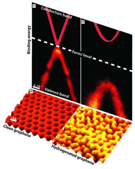
To investigate the electronic effects of hydrogen adsorption on graphene atomic hydrogen was deposited onto graphene supported on an iridium (111) substrate. The bare and hydrogenated graphene surface were then investigated by scanning tunneling microscopy (STM) and angle resolved photoemission spectroscopy (ARPES, see insert for details).
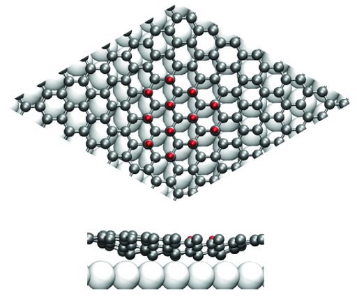
STM images of the graphene surface after hydrogen exposure show that the hydrogen atoms arrange into clusters in an ordered pattern, see Fig. 2b. In the image, areas covered with hydrogen are depicted as bright yellow protrusions. This patterning is caused by the interaction between graphene and the iridium substrate. Theoretical calculations show that graphene can rearrange such that the carbon atoms bind alternately to a hydrogen atom above the graphene layer and an iridium atom below the layer. This arrangement is shown in the model in Fig. 3. Since every other carbon atom is only situated right above an iridium atom on some areas of the surface, this arrangement can only be realized in these regions and hence hydrogen atoms will prefer to bind here. As a result hydrogen adsorbs into the patterned structure displayed in the STM images.
To investigate the effect of this patterned hydrogen adsorption on the electronic properties of graphene ARPES measurements were performed on the clean and hydrogenated graphene surfaces. The results are remarkable and are displayed on top of the STM pictures. The bright curved bands are the occupied electronic states (the valence band) as probed by ARPES. The solid red lines in the figures indicate the expected position of the unoccupied electronic states (the conduction band). While, the band structure of clean graphene is well known, the exact position and shape for hydrogenated graphene is unknown.
For the clean graphene a characteristic cone shaped band is observed and the valance band goes all the way up to the Fermi level. Free standing graphene is a semi metal, meaning that there is no opening between the valance band and the conduction band (which meet at the Fermi level). The band structure of graphene on iridium is very similar to the band structure of free standing graphene; only small gaps in the valence band are seen due to the interaction with the substrate. Therefore graphene on iridium is an ideal system to study fundamental properties of graphene.
After exposing the graphene surface to atomic hydrogen, the band structure changes drastically. The most obvious and interesting change is that a global bandgap is opened, Fig 2d. The absolute value of the bandgap cannot be determined from the ARPES measurements since it only probes the filled states, but it can be determined, that the gap is at least 0.45ev (the energy difference between the Fermi level and the top of the valance band). A bandgap of this size is sufficient for real applications.
The physical origin of the hydrogen induced bandgap opening in graphene is a confinement effect. In clean graphene the valence electrons are highly delocalized, but when hydrogen is adsorbed onto the surface a barrier is created for the delocalized electrons in the surrounding clean areas. Consequently, due to the wave properties of electrons, only certain energies are allowed for electrons confined in the nano sized areas without hydrogen. It is this confinement effect that leads to the observed global band gab opening and opens up the possibility of using graphene as a new material for integrated circuit fabrication.
