RESUME
In this Mid-Term Report we present the results of Project No 298932 (NoVoSiP) obtained during the first year of implementation. At the beginning stage of the project a range of MBE growths and magnetron sputterings were carried out to prepare initial samples with thin SiGe and SiSn strained layers of different alloy composition and thickness followed by different treatments (carbon, helium and hydrogen ion implantation, hydrogen plasma treatment, thermal annealing etc.). Ion implantation was used for injection of dopant atoms as well as point defects in the strained layers. The defects were investigated by transmission-electron microscopy (TEM), dopant depth profiling by secondary-ion mass spectroscopy (SIMS), optical properties by using Raman scattering and optical reflectance measurements.
Using TEM in plan-view and cross-section modes a wide range of structural investigations were carried out. Formation and evolution of growth-, irradiation-, and thermal treatment-related defects were monitored as a function of treatment conditions. It is found that depending on the treatment regime and strain situation, primary defects (interstitials and vacancies) are transformed into nano-voids, platelets and (or) dislocations. We also report on redistribution and segregation of carbon and tin atoms, and structural transformations in strained multi-layered samples after deposition, implantation and thermal treatment in different conditions.
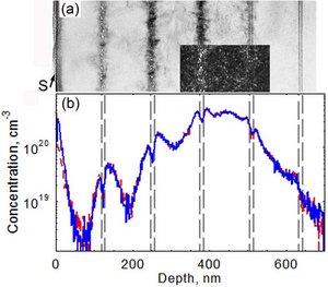
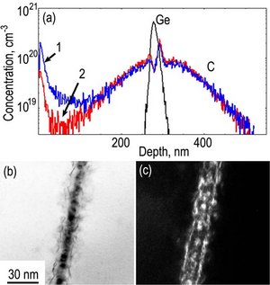
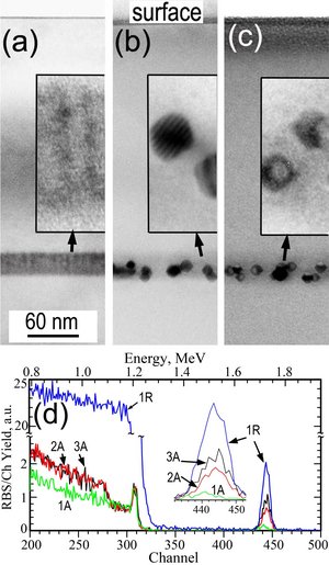
A strong redistribution of dopants in the regions of strained SiGe layers is reported for hot implantation of carbon in the multi-layered Si/SiGe. Carbon atoms are accumulated in the interface region of Si layers, also resulting in nonhomogeneous defect distribution: The density of structural defects is significantly higher in the regions around Si/SiGe/Si interfaces as compared to neighboring central parts of the layers. TEM studies show formation of plate-like defects, stacking faults and thin carbon-related flakes distributed along Si/SiGe interfaces. Raman spectra reveal peaks at 1600 and 2700 cm-1 which might be associated with carbon-related phases. In-diffusion of carbon and retardation of Sn precipitation happen in the case of high temperature carbon implantation of strained Si/SiSn/Si samples. Complicated pictures of spectral oscillation of optical reflectance are obtained in the Si/SiSn and Si/SiGe samples which reflect light interference in the multi-layered structures. The results are discussed taking into account different distribution of damages in the structures.

Publishable summary
In the project No 298932 (NoVoSiP), self-organized formation of nano-voids and nano-dots in strained Si/SiGe/Si and Si/SiSn/Si layered structures are carried out to modify and investigate the structural and optical properties of crystalline silicon for further possible improvement of light harvesting in silicon-based photovoltaic devices. The basic principle for self-assembling of nano-voids and nano-dots in Si is based on the ability of compressively strained SiGe and SiSn alloy layers, incorporated in a Si matrix during epitaxial growth, to collect irradiation-induced vacancies or small-sized molecules followed by thermally activated evolution into voids.
Molecular beam epitaxy, magnetron sputtering or chemical vapour deposition are used for production of strained Si/SiGe/Si or Si/SiSn/Si structures. These structures are then irradiated with light ions (hydrogen, helium or carbon ion implantation, hydrogen plasma treatment etc.) and annealed by pulsed or furnace thermal treatment for the self-assembled formation of voids, strictly adjusted within the compressively strained SiGe or SiSn layers. The void-containing layers are additionally used as templates for segregation and self-assembling of metallic nano-shells, nano-dots, and carbon nano-flakes.
Ion implantation and hydrogen plasma treatment are used for injection of dopant atoms as well as point defects in the strained layers. The defects are subsequently investigated by transmission-electron microscopy (TEM), dopant depth profiling by Rutherford backscattering/channeling (RBS/Ch), secondary-ion mass spectroscopy (SIMS), and the optical properties by Raman scattering, reflectance/transmittance, and photocurrent measurements. Using TEM in plan-view and cross-section modes a wide range of structural investigations have been carried carried out. The formation and evolution of growth-, irradiation-, and thermal treatment-related defects are monitored as a function of treatment conditions. It is found that depending on the treatment regime and strain situation, primary defects (interstitials and vacancies) are transformed into nano-voids, platelets and (or) dislocations. We also report on redistribution and segregation of carbon and tin atoms, and structural transformations in strained multi-layered samples after deposition, implantation and thermal treatment in different conditions.
The following main results have been achieved during the first 2-year period of the project:
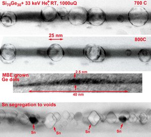
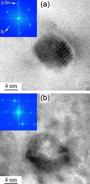
- b- to a- phase transformation is observedin the Sn precipitates as a result of nano-void formation. Self-assembling of spherically shaped voids in nanometer size strained Sn precipitates takes place after high-temperature He+ ion irradiation of Si/SiSn/Si layered structures. The structures will be further investigated for plasmonic applications during the second period of the project.
- Segregation of carbon atoms and formation of carbon nano-flakes has been observed and studied in strained multilayered Si/SiGe/Si structures after MBE growth, carbon ion implantation, and thermal treatment. Anomalous redistribution of the implanted carbon atoms is demonstrated around the strained SiGe/Si layers which results in carbon accumulation on the Si side and depletion on the SiGe side of the structure. Raman spectra reveal peaks at 1600 and 2700 cm-1 which might be associated with carbon-related multi-layered graphen-like phases.
- Carbon related suppression of tin precipitation and elimination of dislocations in supersaturated molecular-beam epitaxial grown SiSn alloy layers is established in the SiSn layers after carbon implantation and high temperature thermal treatment. Strain-enhanced separation of point defects and formation of dopant-defect complexes are suggested to be responsible for the effects. The possibility for carbon assisted segregation-free high temperature growth of heteroepitaxial SiSn/Si and GeSn/Si structures is argued.
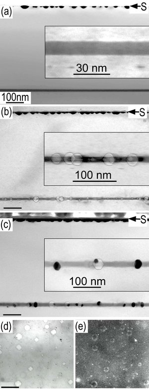
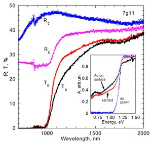
- A gettering-based concept of self-assembled formation of metallic nano-shells and nano-particles in the strained Si/SiGe heterostructures is proposed and developed. Due to strain enhanced vacancy accumulation, the voids nucleate and grow exclusively in the SiGe layer. The voids then getter large amount of Au which covers the inner walls of the voids (formation of nano-shells) or precipitates into the void-located nano-particles at different temperature of thermal treatment. Optical measurements of the layers with void-related Au nano-shells show increase of reflectivity and absorption in the infrared spectral range of 800 – 1800 nm. A favourable feature of metallic nano-shells as compared to nanoparticles is their potentially higher resistivity that might be useful in order to overcome the problem of the ohmic dissipation channel for plasmonic excitations. These metallic nano-shells will be further investigated in solar cell structures for demonstration of plasmonic effects.
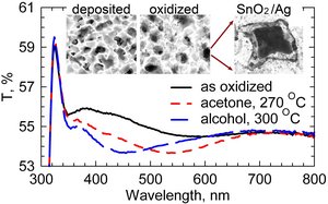
- A plasmonic-related gas sensing effect is demonstrated in the SnO2/Ag nano-composite layers with Kirkendall voids. The nano-composite layers are produced by magnetron sputtering of Sn1-xAgx alloys on a fused silica (FS) substrate followed by thermal oxidation. Silver nano- particles are then segregated into Kirkendall voids in the SnO2 layer. Red- and blue-shift of the silver nanoparticle-related plasmon-resonance peak is monitored in different conditions of gas exposure. The concept of plasmonic based SnO2 sensors is discussed having in mind two main phenomena: First, the ability of metallic nanoparticles to hold plasmonic resonances which depends on the dielectric properties of surrounding SnO2 layer and second, the possibility of space-limited heating of nanoparticles and the neighboring region with light, and in this way to control the chemisorption of oxygen on the sensor’s surface.
The results of the investigations at the first period of the project will be used for preparation of plasmonic structures to enhance the efficiency of Si-based photovoltaic devices, solid-state gas sensors and strained Si/SiGe multilayer plasmonic structures.
FINAL PUBLISHABLE SUMMARY REPORT
The project No 298932 (NoVoSiP) aims at exploring the use of nano-voids and nano-dots prepared as plasmonic structures to enhance the efficiency of Si single-crystalline photovoltaic devices. The main idea behind the production of nanovoids and nano-dots is based on the ability of compressively strained thin SiGe alloy layers, incorporated in a Si matrix during epitaxial growth, to collect vacancies and small-sized molecules followed by thermally activated self-assembling of the nano-voids. The voids are additionally used as templates for self-assembling of metallic nano-shells, nano-dots and carbon nano-flakes. Void containing Si/SiGe strained structures will be further investigated in a photovoltaic device configuration to utilise both near-field and far field effects. The voided structures offer unique possibilities for fundamental investigations.
By combing results from transmission-electron microscopy, Rutherford backscattering spectrometry, secondary-ion mass spectroscopy, optical and photocurrent measurements, the following main results have been obtained after the first 2-year period of the project:
- Self-assembling of spherically shaped voids in nanometer sized, strained Sn precipitates takes place during high-temperature ion irradiation of Si/SiSn/Si layered structure. This is accompanied by a b- to a- phase transformation in the Sn precipitates. The structures are promising for opto-electronic applications (light-emitting devices, photovoltaic devices).
- Formation of carbon nano-flakes in strained multilayered Si/SiGe/Si structures after combined MBE growth, carbon ion implantation, and thermal treatment is found after anomalous carbon redistribution in the strained SiGe/Si layers. Raman spectra reveal peaks at 1600 and 2700 cm-1 which might be associated with carbon-related multi-layered graphen-like phases.
- Carbon related suppression of tin precipitation and elimination of dislocations in supersaturated molecular-beam epitaxial grown SiSn alloy layers is established in the SiSn layers after carbon implantation and high temperature thermal treatment. Strain-enhanced separation of point defects and formation of dopant-defect complexes are suggested to be responsible for the effects. Possible implementation for carbon assisted segregation-free high temperature growth of metastable heteroepitaxial SiSn/Si and GeSn/Si structures is argued. Such structures are promising for optoelectronic applications.
- A new concept for self-assembling of metallic nano-shells and nano-particles in the strained Si/SiGe heterostructures is proposed and developed. Optical measurements of such layers show increased absorption in the infrared spectral range of 800 – 1800 nm. The metallic nano-shells will be further investigated in solar cell structures for demonstration of plasmonic effects.
- A plasmonic-related gas sensing effect is demonstrated in SnO2/Ag nano-composite layers with Kirkendall voids. The nano-composite layers are produced by magnetron sputtering of Sn1-xAgx alloy on fused silica (FS) followed by oxidation at high temperature. Silver nano- particles are then segregated into Kirkendall voids in the SnO2 layer. The spectral shift of the plasmon-resonance peak depends on gas atmosphere and temperature. The concept of plasmonic based SnO2 sensors has been discussed.
The results of investigations carried out in the first period of the project will be used for preparation of plasmonic structures to enhance the efficiency of Si-based photovoltaic devices, solid-state gas sensors, and strained Si/SiGe multilayered plasmonic in opto-electronic devices (light emitting and photodetecting) structures.