Light emission from silicon compatible materials
From a technological perspective, silicon (Si) is one of the most important elements in our daily life. This material can be easily processed in order to obtain a variety of electrical properties, which are exploited in the electronics industry to manufacture basic components (diodes, transistors, etc.). Industrially, one can integrate a huge number of such basic components on a single chip, and thus silicon becomes the crucial element of the entire computer technology.
However, silicon has one major disadvantage - its ability to emit light is very poor. This means that virtually all technological products that involve emission of light (lasers, LEDs, components for fiber-communication) is fabricated from other materials, which are not directly compatible with a silicon chip.
In cooperation with the Semiconductor Group (led by Arne Nylandsted Larsen) at the department of Physics and Astronomy and with the ultra-fast-laser-based materials-processing group (led by Peter Balling), Brian Julsgaard has been in charge of the light emission research from silicon-compatible materials based in particular on time-resolved fluorescence spectroscopy. It is the main objective of the research to contribute to the development of silicon-based materials, which are able to emit light with high efficiency and/or to understand the limiting factors and physical principles behind such light emission.
Germanium islands in silicon
Germanium (Ge) has a bulk bandgap of 0.66 eV, which is lower than that of silicon (1.12 eV). Both Ge and Si have an indirect bandgap, which makes light emission inefficient compared to other decay mechanisms of electron-hole pairs – essentially a result of energy and momentum conservation. However, for nano-structured materials, these conservation laws are partly relaxed and light emission becomes more efficient. This motivates the use of Ge nano-islands inside silicon. Depending on the exact island geometry, the emission energy of the Ge islands can vary but stays below the silicon bandgap. Hence, the emitted light can travel freely inside the silicon and Ge islands present one possible route towards electro-optical integration in silicon.
Recently, we have published two articles related to Ge islands in Si. In [B. Julsgaard, et al., Appl. Phys. Lett. 98, 093101 (2011)], we identify the time scales of various physical processes, which are important for understanding the light emission mechanism. In [B. Julsgaard, et al., to appear in Nanotechnology], we focus more specifically on the Auger-recombination process, which for our chosen island geometries take place on the 10-nanosecond time scale.
Erbium sensitization by silicon
Erbium is a chemical element that can emit light with a wavelength of 1550 nm, which is the standard wavelength in the fiber communication industry. Silicon nanocrystals, silicon-rich silica, or thin silicon layers are able to transfer energy to the erbium, which opens up the possibility of light emission with efficient electrical pumping or broad-band optical pumping as compared to the standard technique of narrow-band laser pumping at 980 nm. Within this field, our research is focused on the basic understanding of the energy-transfer mechanism between the silicon-based sensitizer and erbium receiver ions. In the publication [B. Julsgaard, et al., Phys. Rev. B 84, 085403 (2011)] we identify the characteristic distance dependence of the energy transfer – i.e. how close must an erbium ion be located to the silicon for the energy transfer to be possible. The answer is 0.2 nanometers, which in practice means that the atoms must be in contact with each other. To achieve this result, it is important that the erbium-rich material has not been subjected to high-temperature heat-treatments, in order to prevent that erbium ions wander around in the material by diffusion (see [Y.-W. Lu, et al., Appl. Phys. Lett. 97, 141903 (2010)] for details on erbium diffusion in silicon dioxide).
Light from silicon nanocrystals
Apart from the two main areas of research mentioned above, the fluorescence measurements have also contributed to the understanding of spin-decay dynamics in silicon nanocrystals [B. Julsgaard, et al., Appl. Phys. Lett. 95, 183107 (2009)].
Equipment
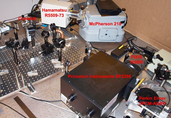
The time-resolved fluorescence measurements exploit a 1 kHz amplified Ti:sapphire laser system at 800 nm with 100 fs pulse duration for optical excitation. Most experiments employ a BBO crystal for frequency-doubling this laser light to 400 nm. Samples can be cooled to 16 K in a home-built closed-cycle cryostat, and the fluorescence can be detected in the range 350 nm - 1600 nm with a time resolution of 1 nanosecond (using a Hamamatsu R5509-73 photomultiplier or a Perkin Elmer SPCM-AQRH-13 avalanche photo diode, attached to a McPherson 218 or Princeton Instruments SP-2358 spectrometer, respectively). Timing control is undertaken by a FastComTech multiscaler board (P7888-2). In addition, integrated spectra can be measured with a Princeton Instruments PIXIS 100BR CCD camera (up to a wavelength of 1100 nm).
Funding
Brian Julsgaard acknowledges support from the Danish Council for Independent Research – Natural Sciences and from the Carlsberg Foundation. The erbium-related experiments have also been supported by the Danish Council for Independent Research – Technology and Production Sciences.
