
Seeing the band gap in an encapsulated 2D transistor using micro-focused light from ASTRID2
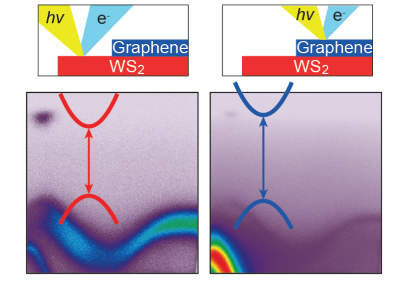
The band gap of a semiconductor completely specifies its function in electronic devices such as the transistors that make our phones and computers work. In a new study led by Chakradhar Sahoo and Søren Ulstrup at IFA, a direct visualization of the band gap in an atomically-thin (2D) semiconductor WS2 was achieved. The study determined the sensitivity of the band gap to the surrounding environment and to the concentration of charge carriers that is induced by a back-gate electrode. This was made possible using advanced photoemission experiments in operando with microscopic spatial resolution at the SGM4 beamline at the ASTRID2 synchrotron light source. It is found that encapsulation under a conductive sheet of graphene surprisingly has a smaller impact on the size of the band gap than the induced carrier concentration in the semiconductor. This observation is explained in terms of screening effects using a theoretical many-body model of the interacting charge carriers in the semiconductor. These findings ultimately aid our fundamental understanding of the electron transport properties of 2D materials, which is critical for optimizing the design of new types of electronic devices.
The study is published in Physical Review Letters as an “Editor’s Suggestion” here: