New two dimensional semiconductor couples selectively to light
Recent paper in ACS Nano reveals surprising electronic properties in the new two dimensional semiconductor rhenium diselenid. Søren Ulstrup of IFA is coauthor.

The toolbox of useful two dimensional materials has a new addition, as Søren Ulstrup from IFA i collaboration with colleagues from a.o. University of Seul in South Korea have succeeded in synthesizing a new semiconducting material named rhenium diselenid, with the abbreviated designation ReSe2. The new material is considered two-dimensional because it consists of a single sandwich of Se-Re-Se atoms with the atoms individually bound in an anisotropic chainlike planar structure. This study has just been published in the renown publication ACS Nano. Apart from documenting the synthesis and the structure of the new material, done a.o. using scanning tunnel microscopy (STM), this study also shows that the material has som quite special electronic properties.
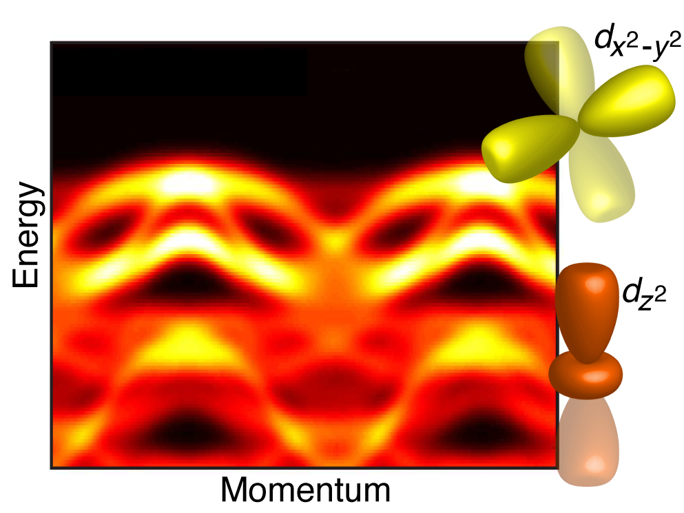
By utilizing synchrotron radiation and the photoelectric effect the researchers have measured the electronic quantum states of the valens bands in ReSe2. They appear to be significantly different from hitherto known 2D semiconductors, as all the lowest state energies respond the strongest to radiation polarized in the same plane as the material. Due to this observation and theoretical calculations it is concluded, that these valens bands primarily are caused by the dx2-y2 orbitals in rhenium, while the electronic higher state energies are linked to the dz2 orbitals.
From this it can thus be deduced that ReSe2 is absorbing light in an extremely selective way, dependent on the energy and polarization of the light. This makes studying the interaction between light and matter in this material especially interesting from the point of view of basic science alone. You could also imagine a combination of ReSe2 and other 2D materials by stacking them like LEGO bricks, in order to combine the selective absorption of light in ReSe2 with some advantageous electric conductivity in a neighbouring layer; thus building up electronic components having unique optical properties.
The full paper in ACS Nano is available here.
