
Studenterkollokvium - Eoghan Rattigan: Two Photon Lithography
Oplysninger om arrangementet
Tidspunkt
Sted
Fys. Aud.
Eoghan Rattigan
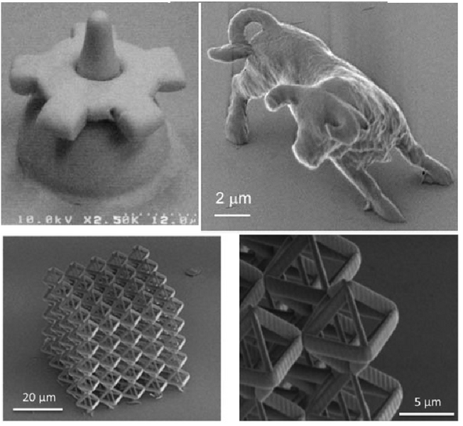
Two Photon Lithography
Supervisor: Jeppe Vang Lauritsen
Date student colloquium: 15/05/17 kl. 14:15
Currently photolithography is the standard method of building electronic devices in a combination of etching, sputtering and curing of photoresists in a layer by layer process. However this method is limited to planar dimensions by this layer by layer process. By focusing high intensities of light of twice the wavelength required to cause curing of the photoresist (2λ), polymers can be generated by the process of two photon absorption (TPA). The photoresist is transparent to light of 2λ wavelength allowing the light to probe deep into the material. Focusing the beam into a tight spot size achieves localised high intensities, where TPA can occur. Scanning this focus point over the surface allows 3-Dimensional structures to be built up from the substrate. This 3D structure can be used as the framework for building 3D electronics.